
Revolutionizing Photonics: Discover the Game-Changing Potential of Perovskite Waveguides!
perovskite waveguides photonics
Perovskite Waveguides: Game-Changing Crystals for Advanced Photonics
Researchers have engineered perovskite crystals poised to transform optical technologies, enabling efficient, room-temperature operations in devices critical for advanced signal processing.
The potential for revolutionizing both classical and quantum signal processing through integrated photonic circuits at room temperature, combined with optical nonlinear effects, is immense.
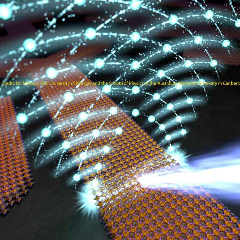
In a collaborative effort involving the University of Warsaw’s Faculty of Physics and other esteemed institutions from Poland, Italy, Iceland, and Australia, scientists have successfully fabricated perovskite crystals with meticulously defined shapes, ideal for applications in nonlinear photonics such as waveguides, couplers, splitters, and modulators.
This groundbreaking research, detailed in Nature Materials, elucidates the creation of these novel structures and the remarkable edge lasing phenomenon.
This phenomenon, in particular, is linked to the formation of an exciton-polariton condensate—quasiparticles that exhibit dual characteristics of light and matter.
Advancing Optical Applications with Perovskites
Professor Barbara Piętka, from the University of Warsaw’s Faculty of Physics and a key figure in the research initiative, highlights perovskites’ versatility, which spans from polycrystalline layers and nano- and micro-crystals to bulk crystals. Their utility ranges from solar cells to lasers.
Notably, materials like CsPbBr3 (cesium-lead-bromide) are exemplary semiconductors for optical applications, owing to their high exciton binding energy and oscillator strength.
These properties facilitate enhanced light interactions, substantially reducing the energy required for nonlinear light amplification.
Pioneering Crystal Synthesis Techniques
Researchers employed reproducible and scalable synthesis methods to craft perovskite crystals with precise dimensions and shapes.
A microfluidic approach was utilized, where crystals are cultivated from a solution within narrow polymer molds, imprinted with any desired shape.
Controlling the solution concentration and growth temperatures in an environment saturated with solvent vapors was essential.
This method, combined with the use of nearly atomically smooth gallium arsenide templates—crafted using electron-beam lithography and plasma etching under the leadership of Anna Szerling at the Łukasiewicz Research Network – Institute of Microelectronics and Photonics—yielded high-quality single crystals.
Consequently, CsPbBr3 crystals can be shaped into various forms, from simple corners to smooth curves, marking a significant advancement in crystalline material science.
These crystals can be fabricated on any substrate, enhancing their compatibility with existing photonic devices.
Mateusz Kędziora, a doctoral student at the University of Warsaw and the paper’s first author, who developed the crystal synthesis methods, remarks on the high quality of these crystals.
They form Fabry-Pérot resonators on their walls, enabling the observation of strong nonlinear effects without the need for external Bragg mirrors.
This advancement holds promise for the integration of these materials into photonic circuits.
Breakthroughs in Polaritonic Lasing and Condensate Formation
The revelation of polaritonic lasing from microwire interfaces and corners marks another significant breakthrough.
Professor Piętka explains that the wavelength of emitted light is altered due to strong light-matter interactions, signifying the emission results from a non-equilibrium Bose-Einstein condensate of exciton-polaritons.
This is not conventional lasing due to the Purcell effect (weak coupling) but rather emission from a condensate within the strong light-matter coupling regime.
Dr. Helgi Sigurðsson from the University of Warsaw’s Faculty of Physics and the University of Iceland’s Science Institute in Reykjavik, adds that the high coherence between different signals emitted from the edges and corners, verified through far-field photoluminescence and angle-resolved spectroscopy, indicates the formation of a coherent, macroscopically extended polariton condensate.
Additional confirmation of nonlinear effects comes from the observed energy increase with the rising population of a given mode, known as blueshift, resulting from interactions within the condensate.
The unique properties of perovskite structures enable the condensate to travel significant distances within the crystals, with emitted light propagating through air gaps to neighboring structures.
Implications for Future Photonic Devices and Technology: perovskite waveguides photonics
Dr. Andrzej Opala from the University of Warsaw’s Faculty of Physics and the Institute of Physics at the Polish Academy of Sciences, a principal author and the theoretical model’s developer, notes that simulations reveal how naturally formed resonators for light modes and scattering influence emission from crystal edges and bends.
Professor Tomasz Czyszanowski from Lodz University of Technology, an expert in photonic and laser structure simulations, explains that by solving Maxwell’s equations in three-dimensional structures with intricate shapes, they visualized photonic modes and illustrated how their image forms in the far field.
These discoveries pave the way for compact “on-chip” systems capable of handling both classical and quantum computing tasks.
Professor Michał Matuszewski from the Center for Theoretical Physics at the Polish Academy of Sciences predicts that these findings will lead to future devices operating at the single-photon level, integrating nanolasers with waveguides and other components on a single chip.
Prospects for Integrating and Commercializing Perovskite Photonic Technologies
Perovskites are poised to play a pivotal role in advancing optical technologies, with the breakthroughs made by physicists from UW significantly enhancing the potential for utilizing perovskite crystals in room-temperature nonlinear photonics.
Furthermore, the developed structures may be compatible with silicon technology, bolstering their commercialization prospects.
Reference
“Predesigned perovskite crystal waveguides for room-temperature exciton–polariton condensation and edge lasing” by Mateusz Kędziora, Andrzej Opala, Rosanna Mastria, Luisa De Marco, Mateusz Król, Karolina Łempicka-Mirek, Krzysztof Tyszka, Marek Ekielski, Marek Guziewicz, Karolina Bogdanowicz, Anna Szerling, Helgi Sigurðsson, Tomasz Czyszanowski, Jacek Szczytko, Michał Matuszewski, Daniele Sanvitto, and Barbara Piętka, 19 August 2024, Nature Materials.